Electronics Designing & Processing
Description
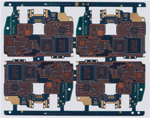
Product name: Handheld electronic device main board
low cost pcb fabrication
Characteristic
1. the blind buried structure is complex. first order HDI:
Blind L1-L2. L5-L6
Buried L2-L5
Through hole L1-L8
2. multiple pressure. heavy copper;
3. laser drilling blind holes;
4. the line width is small. and the etching is difficult;
5. pressing. line. drilling accuracy requirements;
6. a number of times to reduce the surface of copper.
manufacturing pcb china
Specifications
Layer count: 6
Board thickness: 1.0mm
Base materials: FR4 S1000-2
Finished size: 212*170mm
Surface finish: Immersion+OSP
Line width/line space: 3/3mil
Minimum hole: 0.10mm
Solder resist color: Light blue
inner layer H OZ outer layer 1 OZ
Read More
Previous
High frequency antenna board...
China PCB Win Technology Co.,Ltd
Prototype PCBs, Quick Turn PCB, Middle-Low Volume PCBs, Special Technology PCBs, Aluminum PCBs, Custom Printed Circuit Boards
Address: JinYuan Building B-509,XiXiang Road No.300, XiXiang, Bao'an,ShenZhen,China,
ShenZhen, Guangdong
China, 518101
Tel: +86-755-23310576
Fax: +86-755-23310585
